Klipsch Promedia V2.1 Amplifier
Block and Interconnect Diagrams
This is the Klipsch ProMedia 2.1 computer speaker system that began production in 2000. It has two satellite speakers with a control pod on one of them, and a sub woofer that has the amplifier circuits inside with the speaker.
A headphone jack and a line-in jack are included in the control pod together with the main- and sub-woofer-volume controls.
The subwoofer has one side-firing 6.5" long-throw fiber composite cone speaker in a bass reflex tuned MDF box. Driving the speaker is a Class D amplifier that puts out 50 watts @ ? 7% THD from 40- to 100-Hz. Maximum burst power is 200 watts @ ? 1% THD.
At a crossover frequency of 100Hz the satellite speakers kick in. They each have a 0.75" poly compression driver tweeter for frequencies above 5kHz, a 90° x 40° high frequency horn, a 3" long-throw fiber-composite cone woofer in an ABS plastic case. Pumped up by two linear A/B amplifiers, the satellites join the subwoofer to give a total frequency response of 31Hz to 20kHz.
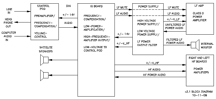
Block diagram of Klipsch Promedia V2.1 System
|
Below are the interconnections for the system. The control pod and the satellite speakers shown are separate units; all other connections are internal to the subwoofer box.
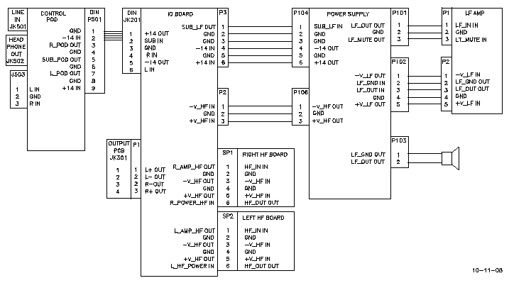
Interconnect diagram of Klipsch Promedia V2.1
|
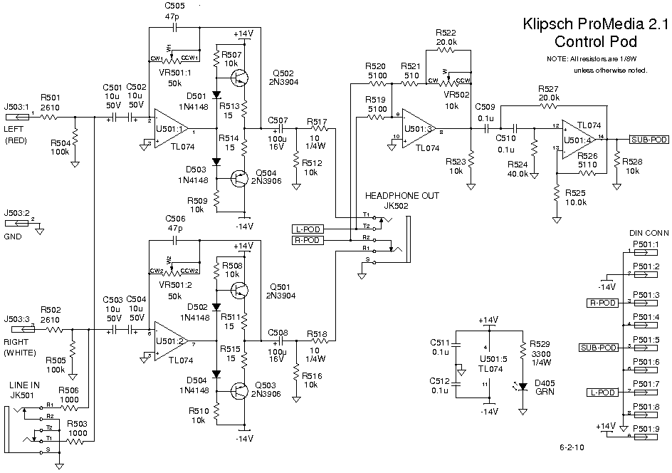
Control Pod
The control pod receives the left and right audio mini-jack input, provides an auxiliary input and headphone output, and mixes the input signals into a summed subwoofer signal. The signal is then buffered by an op amp with a discrete-component output stage (providing a robust headphone amplifier) and then sent to the I/O board through a DIN cable. The signals are also mixed together to create a subwoofer signal with level control, and sent through a high-pass, second-order, Sallen-Key filter before leaving the control pod PCB. When headphones are plugged in the signal is broken and the front channel signal does not leave the control pod PCB.
When the power switch is turned on, a LED glows green. For all three audio signal paths, volume control is produced by changing the amount of feedback around an op amp. Although it works, this is a poor design choice.
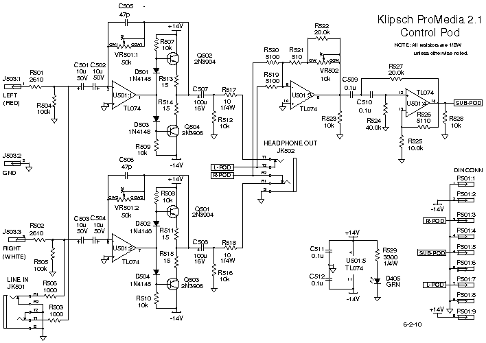
Schematic diagram of Control Pod
|
The diagram below for the V2.1 DIN plug was taken from Klipsch forum postings that I believe are correct. I have not verified it, but I have not found any posts disputing its accuracy. The pin numbers on these diagrams don't conform to the DIN standards.
These diagrams are shown looking at the mating side of the plug pins and not the soldered side.
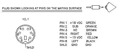
2.1 DIN Plug Wiring Diagram
|
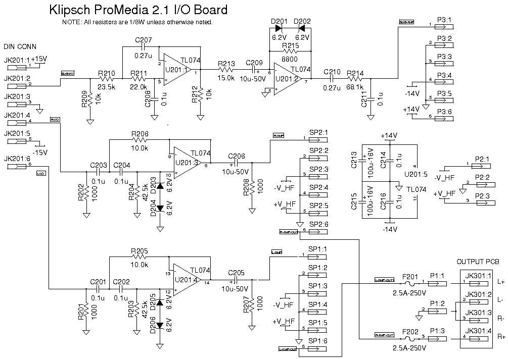
I/O Board
The I/O board receives audio signals for each satellite speaker and sends it through a 2nd order Sallen Key high pass filter. The audio is then AC coupled and sent to the HF amplifiers which are soldered directly to the I/O board by the SP-1 and SP-2 headers. The HF amplifier signals also leave SP-1 and SP-2, are fused, and then sent through P1 to JK301, a spring clip, to connect to the satellite speakers. The subwoofer signal is low-pass filtered with a second-order, Sallen-Key filter, AC coupled and buffered while having its amplitude nearly halved, and then filtered again by a passive first-order filter before being sent through ribbon cable P3 to the LF amplifier (via the power supply PCB).
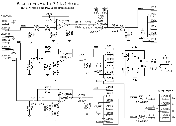
Schematic diagram of I/O Board
|
HF (Satellite) Amplifier Board
The satellite speaker amplifiers are quite basic linear amplifiers. Although the boards have different reference designers, the copper, components, and everything but the silkscreen is identical between the boards. Q1 and Q2 are a long tail pair forming a differential input stage and fed by constant current source Q4. Q5 is a constant current source for the driver transistors Q7 and Q8, which receive the audio signal by Q5. The output transistors are Q9 and Q10, while Q6 is a bias transistor mounted on the heatsink between the output transistors. R18 and R19 are jumper wires. C7 and R20 are a simple zobel network. The output transistors have mica wafers between their tabs and the mounting plate.
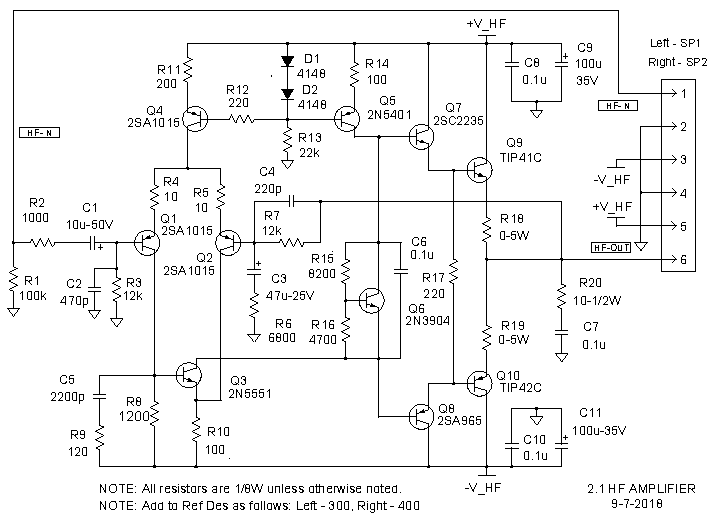
Schematic diagram of HF Amplifier Board
|
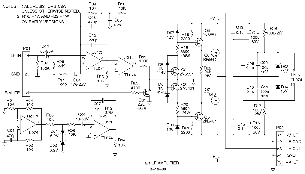
LF (Subwoofer) Amplifier Board
The subwoofer amplifier is a switching (class D) amplifier. It uses a basic, well-known triangle modulator. U1:2, along with zener diodes D1 and D2, create a roughly square wave. That signal is integrated by U1:1 into a triangle wave and sent to the modulator. The input audio signal is mixed with the feedback by U1:3 and then compared with the triangle wave by U1:4. The PWM signal is level shifted and sent to the drivers and output FETs. The output filter is on the power supply PCB.
The subwoofer amp power supply rails are used to create roughly +/-15V rails for the quad op-amp using zener diodes. Alumina is used to isolate the amplifier FETs from the mounting plate. Q1 could be used to shut down the amplifier by grounding the PWM signal leaving the modulator, but the control circuitry for Q1, which would be on the power supply board, is completely absent.
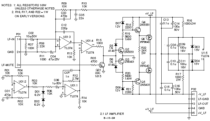
Schematic diagram of LF Amplifier Board
|
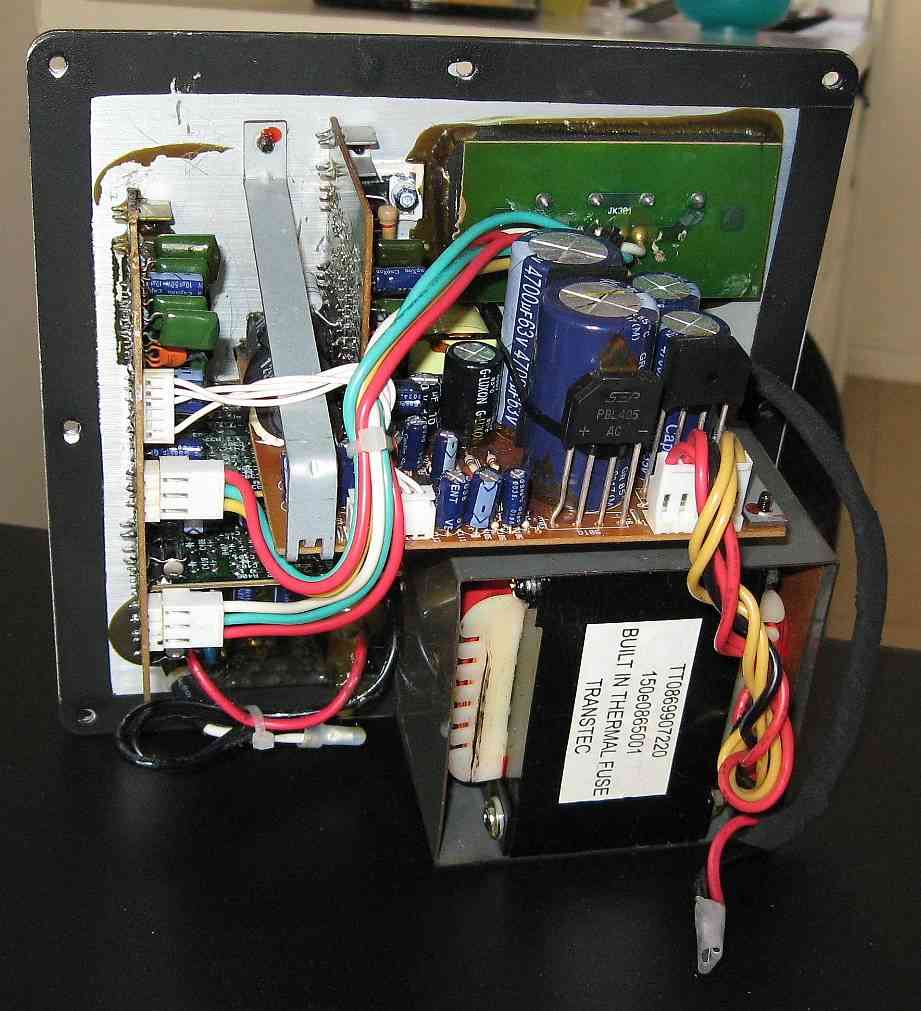
Power Supply
The power supply is a simple linear power supply. AC line voltage runs through the power switch and fuse before reaching the transformer primary. The transformer is a laminate E-core. Bridge rectifiers create +/-26V for the HF (satellite) amplifiers and +/-50V for the LF (subwoofer) amplifier. The HF amplifier rails are also used to create +/-14V housekeeping voltages via discrete linear regulators.
P104 is a ribbon cable connecting to the I/O board. It carries housekeeping voltage to the rest of the circuitry and receives the subwoofer audio signal which is sent to P101. P102 is the high voltage connector for the LF amplifier. The high voltage PWM signal from the LF amp comes in through P102:3 and is filtered by a 4th order filter to leave the amplified audio signal. A relay blocks the LF audio output from reaching the speaker until the AC line voltage surpasses about 70VAC and there is no DC present on the LF output.
The relay control circuit checks the HF rail voltage, the AC line voltage, and the LF amplifier output. The HF amplifier rails are rectified and divided at Q104's base, which acts as a voltage buffer/reference. R102 biases D102 and turns Q101 on, which energizes the relay's coil. Until the AC line voltage gets above 70VAC, Q104 pulls down on Q101's base, which breaks the LF audio output connection to the speaker. If DC is present on the LF output, Q102 and Q103 can detect either polarity of DC and pull down on Q101's base to break the LF audio output connection to the speaker.
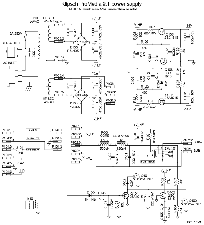
Schematic diagram of Power Supply
|
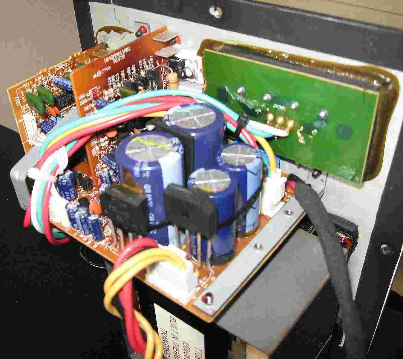
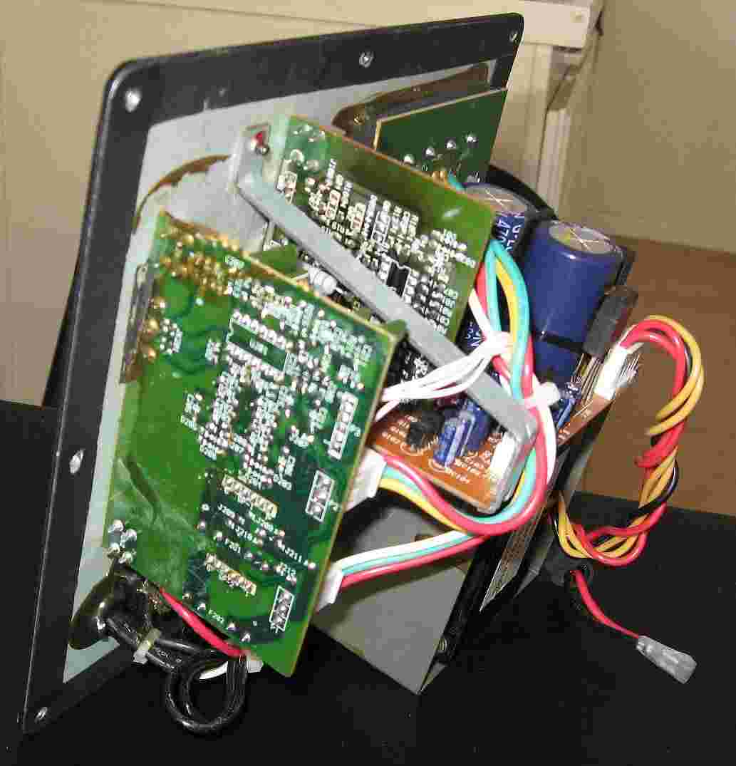
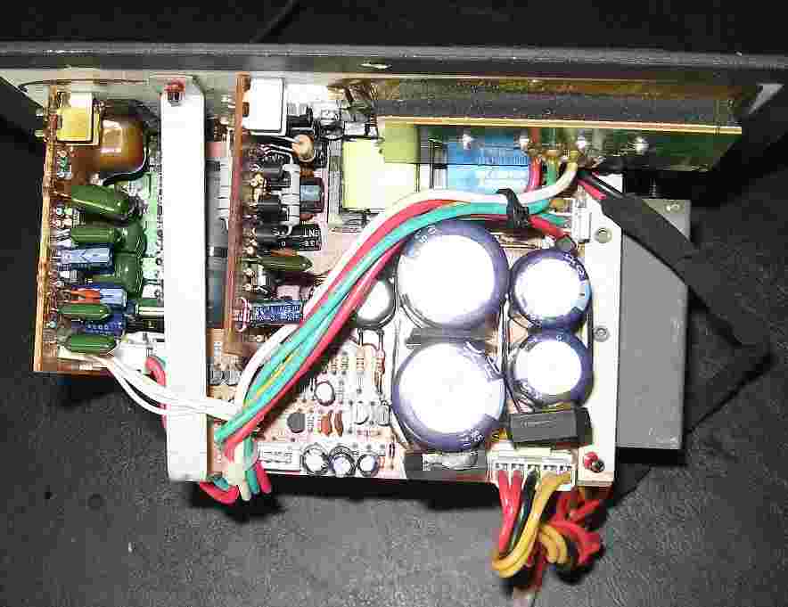
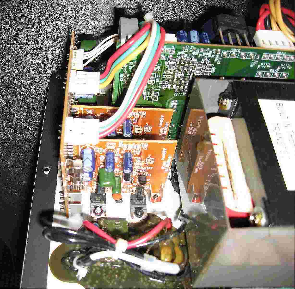
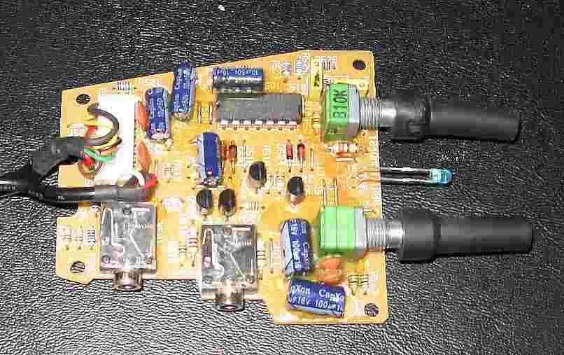
Photo Gallery
Copyright Dale Thompson,
September 10, 2008 through
last revision on September 7, 2018